logo
Main Theory Technology Analitic Application Contacts
ru

Technology
Technology ...
Electroluminescence
Electroluminescence ...
Measuring
Measuring ...
Panels
Solar Panels ...
Solar charger
Solar charger ...
The technology of silicon solar cells production
technology
The raw material is boron doped "solar" silicon wafer with resistivity in 0.5-3 Ohm*cm, thickness in 200 mkm and 125х125 mm or 156х156 mm dimensions. The following steps should be done to produce solar cell:
  • saw damage etching*;
  • texturing;
  • chemical treatment;
  • phosphorus diffusion;
  • phosphorous silicate glass (PSG) removing;
  • antireflection coating (ARC);
  • screen printing of contacts;
  • contacts firing;
  • laser isolation;
  • measurement.
* optional.
The wafer
the wafer (REM)
As cut wafer has serious damages on it’s surface. There are a lot of cavities, micro cracks and hills – it is saw damage layer, which was created during wafer production (sawing ingots). This surface leads to very high surface recombination velocity which is fatal for solar cell. The chemical etching of saw damages and/or texturing are used to fix this problem.

At the picture (left) is showed a small zoomed part of as cut wafer surface. This picture was took by electronic scan microscope.

Saw damage etching
Saw damage etching (SDE) is used for smoothing surface and dirty removing. Usually SDE is performed in hot alkaline solution.
ТНС1 ТНС2

At these pictures are showed zoomed parts of wafer’s surfaces after SDE. Lighter SDE is showed left. Deeper SDE is showed right.

Texturing
Texturing the surface of the wafer is performed for a significant reduction of the reflection coefficient and surface recombination velocity. The mono wafer texturing are performed in the anisotropic etching alkaline solution, resulting in the formation four facet pyramids, the apex of which is directed upwards. Meanwhile the texturing of multicrystalline wafers can be done as well by anisotropic etching alkaline solution as by isotropic acid solution. Due to multicrystalline wafer has not uniform crystalline orientation it is impossible to make the upwards directed pyramids by anisotropic alkaline etching. A lot of craters can be formed on silicon surface by using acid isotropic etching independently on crystalline orientation.
texture planar texture angle

At thess pictures are showed zoomed small area of wafer surface after texturing. Top view is showed left and angle view is showed right.
Phosphorous diffusion

The diffusion is a main step in solar cells production. It is used for creating p-n junction which divides photo generated charge carriers. The chemical cleaning must be done before diffusion to protect silicon lattice from impurities which can lead to defects in p-n junction which drops solar cell parameters.

The phosphorous diffusion usually is realized in tube diffusion furnace at atmospheric pressure and temperature 800-900oC. The POCl3 is used as phosphorous source. The diffusion process can be divided onto several steps listed below:

  • Silicon oxidization with phosphorous silicate glass (PSG) formation on the silicon surface;
  • Phosphorous diffusion from PSG into near surface layer;
  • Phosphorous diffusion from near surface layer into bulk.

Thus, the electronic conductivity (n-type) layer is formed on whole surface of wafer. This layer is called emitter. The front emitter has two functions: p-n junction formation with base and transmission electrons to metal fingers.

before diff. -> after diff.

Emitters which are located at edges and back side is undesirable because it lead to internal shot circuit. Therefore they should be removed at next steps to isolate front emitter from back side and edges.

Antireflection coating

The antireflection coating (ARC) is used to decrease reflection from front surface and for it passivation. Also it make nice view of solar cells. Usually ARC consists from silicon nitride film with refractive index n= 2 - 2.15 and thickness around 70 - 80 nm.

После дифф. -> После АОП

In most cases the antireflection coating deposits by plasma enhanced chemical vapour deposition (PECVD) in vacuum chamber at 350-450oC using silane (SiH4) and ammonia (NH3).

Solar cell color is depends on ARC optical thickness and spectrum of light. So the color of the same solar cell can be different in dependence on sunny weather or not, light from sun or from lamp and so on. This phenomena describes by interference low on which principle of ARC is based.

Contact formation

The metal pastes are deposited on to wafer surfaces by screen printing to form metal contacts. Usually it does in this sequence:

  1. printing of front silver contacts (grid with 2-3 busbars);
  2. drying;
  3. printing of rear silver/silver-aluminum contacts (2-3 busbars);
  4. drying;
  5. printing of rear aluminum contact (full area);
  6. drying;
  7. fast firing in furnace

The screen printing of contacts is extrusion of some value of metal paste onto wafer surface throw openings in screen. Generally metallic paste consist from metallic particles, binding material, solvent and glass. The glass play quite important role especially during front contact formation.

After drying the thick film of metallic paste becomes hard enough for next handling (printing or firing). The binding material is evaporated at the beginning of firing process. Then the glass solves the ARC under front contact. The aluminum at the rear side forms back surface field (BSF) and mirror.

Isolation
After conventional diffusion the n-type region cover all surface of silicon wafer even at the edges. To prevent shot circuit between front and rear contact it is necessary to remove from edges or/and from back side n-type layer. This task can be done in different ways. The most popular of them are described below.

Plasma etching of edges

PCE The etching of edges by plasma-chemical reaction is a batch operation. A light squeezed stack of wafers moves to a vacuum chamber for plasma etching at room temperature in the fluorine contained atmosphere. In this case the fluorine ions bind to silicon atoms form thus gas SiF4 which is easily removed from surface to vacuum pump. It leads to disappearance parasitic n-type layer from edges.

Liquid etching

LE The silicon wafer is placed onto roll system which moves the wafer to the etching solution for liquid etching of parasitic n-type layer. It is important that solution does not take front surface to prevent removing front side emitter. Thus only emitter from back side and edges can be removed completely. It results to very good isolation.

Laser isolation

ПХТ The laser beam is scanned at front (some times at back) surface near the edges to make grooves between edge and front emitters. These grooves are formed by explosion some part of material during laser pulses illumination. The depth of the groove is much more then depth of n-type layer so there is no n-channel between front and edge emitters after laser treatment. It also results to very good isolation but it cuts some active part from front side emitter which leads to bit decreasing of shot circuit current and efficiency of cell. Although efficiency lost the laser isolation becomes more popular cause its easy setup and not expensive usage.
Measuring

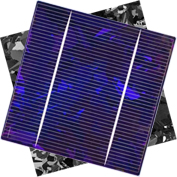
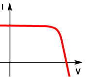
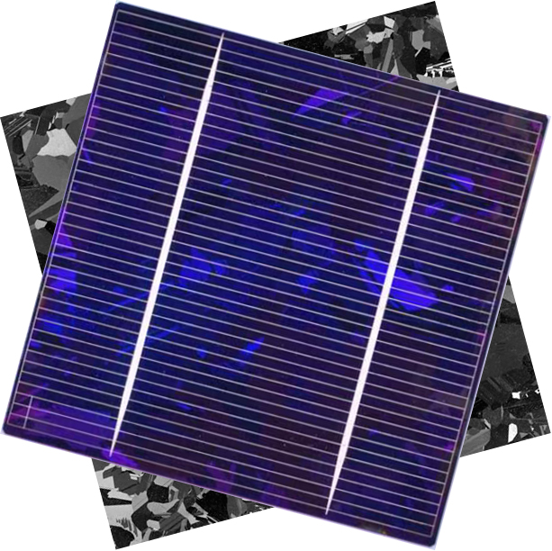
The measuring is a last step in solar cells production. At this operation every solar cell is connected to electronic load and illuminated with light spectrum AM1,5 to obtain the voltage-current characteristic. Then calculates solar cells parameters like shot circuit current, open circuit voltage, fill factor, maximum point power, efficiency, serial and shot circuit resistances and others. The measuring system determines the class of current solar cell and places it into corresponded box.

The silicon solar cell efficiency has strong dependence on temperature. It should be kept in mind that measured efficiency should be recalculated to 25оС before classifying.

Also the great influence on measurement has arrangement of probe contacts and its quantity. It happens because silver busbar has quite high resistance (much higher than copper ribbon which used in assembling modules) and thus can not support uniform load by few contacts. The compromise of this situation is a balanced location of probe contacts or using multiple contacting systems.

An additional information about measuring you can find here.

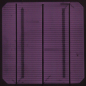
Additionally the electroluminescence imaging should be done to obtain complete picture of solar cell quality. The electroluminescence makes it possible to detect and distinguish most defects of solar cell (cracks, micro-cracks, fingers interrupts, low efficiency regions, higher series resistivity, low lifetime regions, shot circuit etc.) This method is nondestructive which take picture of solar cells by principle “dark region - trouble region”. An additional information about electroluminescence you can find here.

Hosted by uCoz